Welcome to the continuation of our mini-series of blogs about the ESP32 Optoisolated Programmer – PCB Analysis #3. Enjoy!
Panelization
Panelization is a way to reduce the production time of a PCB. To the actual assembly time, which depends on the number of elements, you must also add the time of entry and exit from the assembly machine. This time is completely independent of the number of components. For this reason, production panels are made, consisting of a repeatedly duplicated PCB design.
The size of the panel should be discussed with the company that will assemble the product, because the optimal size of the panel depends on the capabilities of the machines that the company has. On the one hand, the more PCBs in the panel, the better, because the time of entry and exit is spread over a larger number of products assembled at the same time. On the other hand, the larger the panel, the greater the problems with panel stiffness, which can cause the board to vibrate during assembly, the components to shift, and even the panel to fall in the soldering oven.
In addition, a fabrication panel is a way for the board to have a shape other than rectangular. The shape of the board can be absolutely anything, but keep in mind that the more it deviates from a rectangular shape, the more of the panel will have to be cut off later, which will be a waste cost.
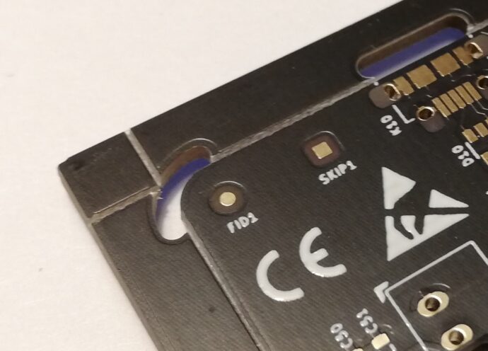
We decided to round the corners of our tiles so they wouldn’t scratch tables and other objects. In the panel frame, we marked the areas to be milled with the curve.
Fiducials
Fiducials are markers that allow the machine to locate the board. We use three types of fiducials:
- Local – these are three points placed in the corners of each board
- Global – these are three points placed on the frame of the panel
- Skip marks – these are markers that allow the machine placing SMD elements to ignore a faulty PCB. The laminate production process is not perfect and sometimes there are defects. However, the defect generally affects a single PCB in the panel, while the rest of the PCBs are suitable for production. To avoid wasting the entire panel, the PCB manufacturer seals or paints a skip mark on the defective board with a marker pen. Before applying the components, the pick&place machine checks all the skip marks and thus determines which boards to apply the components to and which to ignore.
Depanelization
There are various ways to cut a production panel into individual boards after SMT and THT soldering is completed. The most common method we use is the v-cut method. The laminate manufacturer makes scratches on the top and bottom side of the board where the panel is to be cut into pieces. After production, the panel can be split without any tools. The disadvantage of this solution is the residue in the form of protruding glass fibers that must be removed with a file. Larger production batches can be cut with a depanelizer adapted to v-cutting.
Thank you for joining us on this journey about our PCB Analysis. Until the next time!