This post will describe the proposed FPGA application architecture. It is not meant to be a step by step tutorial, rather an overview with an explanation of main modules. For the complete source code refer to WizzDev GitHub repository.
Data flow
First a short description of a data flow in our application.
All data is generated by a dedicated module (for the purposes of this demo this will be either a sine or saw signal generator, but in a real application, it’s usually some sort of sensor with ADC). Samples from each source are 2 bytes wide and are collected at a fixed rate, and then fed to the first FIFO. FIFOs between the modules are needed because of crossing from different clock domains and to provide a convenient way to change the width of data.
From the first FIFO data is fetched by a packet assembler. It prepares a larger portion of data to be send and appends additional info to each packet:
- 32-bit wide ID at the beginning – to enable packets continuity validation by the receiving module,
- 32-bit wide checksum at the end, computed as a sum of previous 32-bit packet segments (including the ID).
So for example: having a packet length of 512 bytes, with 4 sources, each sample takes 2 bytes (16 bits), with 4 bytes (32 bits) checksum and 4 bytes ID, the number of timestamps in one packet will be:
number_of_timestamps = ( (512B - 2*4B) / 2) / 4 = 63
And with a 256 bytes packet and 31 sources it will be:
number_of_timestamps = ( (256B - 2*4B) / 2) / 31 = 4
Packets are then buffered in DDR3 memory where are waiting to be sent by USB module. Again FIFOs are used because of 256-bit data width while reading and writing to memory.
Data generation module
entity source_generator is
    Generic (INPUT_CLK_F : natural := 100e6; -- 100MHz
             TARGET_SAMPLING_FREQ : positive;
             NUMBER_OF_SOURCES : positive);
    Port ( clk : in STD_LOGIC;
           ce  : STD_LOGIC;
           reset : in STD_LOGIC;
           mode  : in STD_LOGIC_VECTOR(3 downto 0);

           data_fifo_out : out STD_LOGIC_VECTOR(31 downto 0);
           data_fifo_re  : in STD_LOGIC;
           data_fifo_count : out STD_LOGIC_VECTOR(8 downto 0)
);
end source_generator;
Entity declaration from source_generator.vhd
This module was written to organize the separate sources and feed their output to the FIFO at a correct order. The number of sources and sampling rate are configurable and can be specified before synthesis (look at demo_top entity’s generics). FIFO that is a part of this module has 16-bit input width (because of 16-bit source samples) and 32-bit output width which is more convenient for a packet assembler.
For this demo generated sources are sine and saw signals alternatively, with increasing frequency (sine) or max amplitude (saw).
E.g. for 4 sources it will be: 1) sine f=10Hz, 2) saw max_amp=2*1024, 3) sine f=3*10Hz and 4) saw max_amp=4*1024.
Packets assembling module
entity data_packet_wrapper is
    Generic (PACKET_LENGTH : positive;
             PACKET_ID_LENGTH : positive;
             CRC_LENGTH : positive);
    Port (
            clk_in :    in STD_LOGIC;
            reset :     in STD_LOGIC;

            data_fifo_out : in STD_LOGIC_VECTOR(31 downto 0);
            data_fifo_re : out STD_LOGIC;
            data_fifo_count : in STD_LOGIC_VECTOR(8 downto 0);


            packets_fifo_we : out STD_LOGIC;
            packets_fifo_in : out STD_LOGIC_VECTOR(31 downto 0);
            packets_fifo_full : in STD_LOGIC

         );
Entity declaration from data_packet_wrapper.vhd
Reads 32-bit slices of data from source generator output FIFO and feeds them to its output FIFO, inserting the new ID at the beginning of every packet, and computed checksum at the end. <!The checksum is computed after each new data is read at the input.> The output FIFO has 32-bit wide input and 256-bit output – so it can be connected directly to DDR3 memory controller bus.
DDR3 memory controller
entity ddr3_fifo_controller is
  Generic (PACKET_LENGTH : positive;
           PACKET_ID_LENGTH : positive;
           CRC_LENGTH : positive);
  Port (
      ui_clk                        : in    std_logic;
      rst                           : in    std_logic;
      -- DDR3 app interface
      ddr3_input_buffer             : out   std_logic_vector(255 downto 0);
      app_addr                      : out    std_logic_vector(28 downto 0);
      app_cmd                       : out    std_logic_vector(2 downto 0);
      app_en                        : out    std_logic;
      app_wdf_end                   : out    std_logic;
      app_wdf_wren                  : out    std_logic;
      app_rd_data_valid             : in   std_logic;
      app_rdy                       : in   std_logic;
      app_wdf_rdy                   : in   std_logic;
      init_calib_complete           : in   std_logic;

      -- data in interface
      packets_fifo_out              : in    std_logic_vector(255 downto 0);
      packets_fifo_re               : out   std_logic;
      packets_fifo_count            : in    std_logic_vector(10 downto 0);
      packets_fifo_valid            : in    std_logic;
      -- data out interface
      fifo_pipeout_we               : out   std_logic;
      fifo_pipeout_full             : in    std_logic;
      -- fifo flags
      ddr3_empty                    : inout   std_logic;
      ddr3_full                     : inout   std_logic;
      fifo_out_write_data_count     : in      std_logic_vector(9 downto 0);
      fill_level                    : inout   integer := 0;

      DEBUG_OUT                     : out     std_logic_vector(7 downto 0)

    );
end ddr3_fifo_controller;
Entity declaration from ddr3_fifo_controller.vhd
It incorporates the Xilinx MIG7 (Memory Interface Generator) which handles the communication with DDR3 chip on a physical layer and simultaneously provides a convenient interface for a designer. A packet FIFO’s output (256-bit wide) is connected to its “data in” port, and another output FIFO (256-bit in, 32-bit out) is connected to its “data out” port. Reading and writing are organized by applying a FIFO-like algorithm to track the read and write addresses, and the fullness of the memory.
USB modules
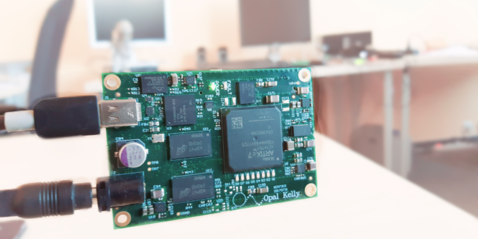
USB communication is handled by Opal Kelly’s FrontPanel Firmware running on a microcontroller connected to the FPGA and a USB socket.
The Opal Kelly FrontPanel HDL modules must be added to the design to enable this feature.
This application utilizes:
okHost (from okLibrary.v), with the first 4 signals connected to physical pins of the FPGA, connected to the USB microcontroller (this pins must be specified in the .xdc constrains file), and the latter 3 which serve as control signals inside the design. This is the most important module that must be instantiated to ensure FrontPanel usage. The rest is optional and depends on your target application needs.
okHI : okHost port map (okUH => okUH,  -- [4:0] input Host interface input signals
                        okHU => okHU,  -- [2:0] output Host interface output signals
                       okUHU => okUHU, -- [31:0] inout Host interface bidirectional sigals
                        okAA => okAA,  --        inout host interface bidirectional signal

                       okClk => okClk, --         output Buffered copy of the host interface clock (100.8 MHz)
                        okHE => okHE,  -- [112:0] output Control signals to the target endpoint
                        okEH => okEH   -- [64:0]  input Control signals from the target endpoint
);
Example of okHost entity instantiation from demo_top.vhd
Blockstrobe pipeOut for sending generated data to PC (USB bulk transfer):
epA0 : okBTPipeOut
    port map (okHE              =>  okHE,
              okEH              =>  okEHx(2*65-1 downto 1*65),
              ep_addr           =>  x"A0",
              ep_read           =>  pipe_out_read,
              ep_datain         =>  pipe_out_data,
              ep_blockstrobe    =>  block_strobe,
              ep_ready          =>  pipe_ready
              );
Example of okBTPipeOut entity instantiation from demo_top.vhd
TriggerIn for receiving control signals that are sent from PC:
ep40 : okTriggerIn
    port map (okHE          => okHE,
              ep_addr       => x"40",
              ep_clk        => ui_clk,
              ep_trigger    => ack_trigg
              );
Example of okTriggerIn entity instantiation from demo_top.vhd
WireIn for another control signals receiving (e.g. reset):
ep00 : okWireIn
    port map (okHE          =>  okHE,
              ep_addr       =>  x"00",
              ep_dataout    =>  ep00wire);
Example of okWireIn entity instantiation from demo_top.vhd
WireOut to provide some additional information channel (in this case sending DDR fill level value whenever requested from PC):
ep21 : okWireOut
    port map (okHE => okHE,
              okEH => okEHx(1*65-1 downto 0*65),
              ep_addr   => x"21",
              ep_datain => control_out_data);
Example of okWireOut entity instantiation from demo_top.vhd
And the last – WireOR, required whenever more than one module that sends out the data are present:
WireOR: okWireOR
    generic map (   N => 2)
    port map (okEH   => okEH,
              okEHx  => okEHx);
Example of okWireOR entity instantiation from demo_top.vhd
Demo_top module
entity demo_top is
    Generic (NUMBER_OF_SRCS : positive := 4;
            SAMPLING_FREQUENCY : positive := 1e4;
            PACKET_LENGTH_BYTES : positive := 512);
    Port (
           -- USB3.0 interface
           okUH     : in STD_LOGIC_VECTOR(4 downto 0);
           okHU     : out STD_LOGIC_VECTOR(2 downto 0);
           okUHU    : inout STD_LOGIC_VECTOR(31 downto 0);
           okAA     : inout STD_LOGIC;

           -- onboard clock
           sys_clkp : in STD_LOGIC;
           sys_clkn : in STD_LOGIC;

           -- DDR3 interface
           ddr3_dq      : inout STD_LOGIC_VECTOR(31 downto 0);
           ddr3_dqs_p   : inout STD_LOGIC_VECTOR(3 downto 0);
           ddr3_dqs_n   : inout STD_LOGIC_VECTOR(3 downto 0);

           ddr3_addr    : out STD_LOGIC_VECTOR(14 downto 0);
           ddr3_ba      : out STD_LOGIC_VECTOR(2 downto 0);
           ddr3_ck_p    : out STD_LOGIC_VECTOR(0 downto 0);
           ddr3_ck_n    : out STD_LOGIC_VECTOR(0 downto 0);
           ddr3_cke     : out STD_LOGIC_VECTOR(0 downto 0);
           ddr3_dm      : out   STD_LOGIC_VECTOR(3 downto 0);
           ddr3_odt     : out   STD_LOGIC_VECTOR(0 downto 0);
           ddr3_ras_n   : out   STD_LOGIC;
           ddr3_cas_n   : out   STD_LOGIC;
           ddr3_we_n    : out   STD_LOGIC;
           ddr3_reset_n : out   STD_LOGIC;

           -- onboard LEDs
           debug_LEDs : out STD_LOGIC_VECTOR(7 downto 0) := (others => 'Z'));
end demo_top;
Entity declaration from demo_top.vhd
This is a top entity where all modules are joined together and connected. Each of its ports must have a corresponding statement in the .xdc constraints file that will define which physical FPGA pin it is assigned to. A few generics that are specified at the beginning lets you configure the resulting design by specifying the number of sources, desired sampling frequency and the packet length. Please refer to the packet structure diagram before playing with these.
One more thing before generating the programming file.
Working with generics
Working with generics is convenient because you can easily change some parameters in one place of the code and then just generate a new bitstream. Going further, a Tcl script can be incorporated to do this automatically. But they can cause some serious errors within the design when carelessly used, especially when the values must obey some specified rules, like in this case.
Therefore the assert statements are useful wherever wrong generic’s values may cause the design to break. They are evaluated during the Synthesis stage and prevent the design to be implemented if the rules were broken. To enable the asserts, the corresponding flag in Synthesis parameters must be checked. To do this go to “Settings -> Synthesis” and make sure that “-assert” is checked. (It’s usually not, so we recommend you do this before synthesizing and implementing the design).
Now you can safely generate bitstream file by clicking “Generate Bitstream” on the left panel. The window can appear informing that the Synthesis is out-of-date. Accept it to run Synthesis, and Implementation once again before the bitstream generation.